


IBM has announced a technological innovation capable of overcoming current barriers to miniaturizing components in computer chips, a challenge that has limited the progress of the semiconductor industry in recent decades.
This new approach paves the way for manufacturing smaller components within integrated circuits, promising to increase the efficiency, performance, and capacity of processors that power everything from mobile devices to high-performance data centers.
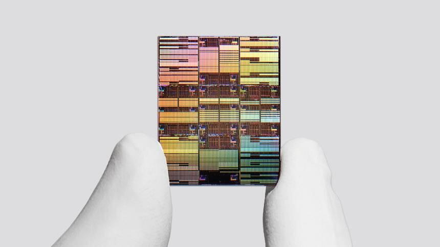
The company described its new production process as being 0.7 nanometers, the first to break the one-nanometer barrier, capable of producing the world's smallest chip. The innovation, presented by IBM, is what the company calls a "nanostack" transistor.
The miniaturization of components is one of the main drivers for the advancement of chips, but the industry faces physical and technical limitations that hinder the continuous reduction in the dimensions of transistors and interconnects.
Traditional technology is approaching a practical limit, known as the "limit of quantum physics," which poses challenges such as electronic interference and thermal dissipation. IBM's solution proposes an innovative method to overcome these barriers, allowing for the construction of smaller structures with greater precision and control.
IBM reported that the new production process can accommodate almost twice as many transistors on a chip the size of a fingernail compared to the previous technology, launched in 2021. This will provide 50% higher computing performance and 70% better energy efficiency.
Both attributes are highly sought after, especially in the race to build data centers focused on artificial intelligence. Energy consumption is a particularly critical challenge.
"Everyone demands more performance, but no one wants to pay for the energy required for it," said Huiming Bu, IBM's vice president in charge of chip research and development, during a presentation to journalists.
Although it was a pioneer in the semiconductor industry, IBM no longer manufactures or sells chips. However, engineers at its laboratory in Albany, New York, continue to develop new technologies to transform silicon wafers into chips—technology that the company generally licenses to manufacturers.
Bu stated that the technology should be ready within the next five years, but declined to reveal which companies might use it. Among the companies that have licensed IBM technologies in the past are Samsung Electronics and Rapidus, a Japanese company.
The new process developed by IBM is still in the early stages of research and development, with no immediate commercial application.
However, it positions the company as a protagonist in the next era of the chip industry, especially at a time when hardware manufacturers and large technology companies are seeking alternatives to continue advancing in computing capacity.
This method could positively impact sectors that rely on more powerful semiconductors, such as artificial intelligence, cloud computing, and connected devices.
IBM's innovation is based on advanced lithography techniques and semiconductor materials, combined with manufacturing processes that increase the resolution and density of components.
This means that it is possible to fit more transistors into a smaller area, increasing chip performance without increasing energy consumption, a crucial aspect for sustainability and efficiency.
The company has been investing in research on materials and processes for chips for years, and this new technology is the result of that continuous effort.
The potential market for this innovation is enormous, considering the growing demand for faster and more efficient chips in sectors such as artificial intelligence, the Internet of Things (IoT), 5G, and high-performance computing.
Competitors in the segment, such as traditional semiconductor manufacturers and specialized startups, are also seeking solutions to overcome the limits of miniaturization, but IBM's approach stands out for its promise of a significant advance in component density.
Despite its potential, the technology faces challenges in achieving commercial scale. These include high implementation costs, the need to upgrade production lines, validating the reliability of chips manufactured using the new method, and adapting design and manufacturing ecosystems. Furthermore, regulatory issues and industry standards may influence the speed of adoption in the global market.
IBM still needs to demonstrate that the technology is viable on a large scale and can be integrated into existing chip manufacturing processes. The transition from the experimental phase to mass production involves significant investments in infrastructure, as well as strategic partnerships with manufacturers and end customers.
Market acceptance will also depend on the company's ability to demonstrate concrete gains in performance, cost-effectiveness, and sustainability.


